Tampere can save Europe’s future with its chip expertise

Tampere is at the forefront of chip expertise in Europe and the world, thanks to the long-term co-operation between the university, research institutes and companies. Tampere already has a European centre of chip expertise, and it will also have one of the five EU chip pilot lines.
Computers, smartphones, cars and pacemakers – our lives today depend on chips. Tampere has been building the foundations of chip expertise for decades. The university, research institutes and companies have conducted a considerable amount of research and development work, even on a European and global scale, so that our current life is possible, not to mention the future.
Among the global political turmoil, chips and chip expertise have become a key symbol of the global race and its dependencies. The COVID-19 crisis, wars and shifts in the superpower relations have revealed Europe’s vulnerability and dependence on the rest of the world. But could Tampere save the whole of Europe from the chip domination of the United States and Asia?
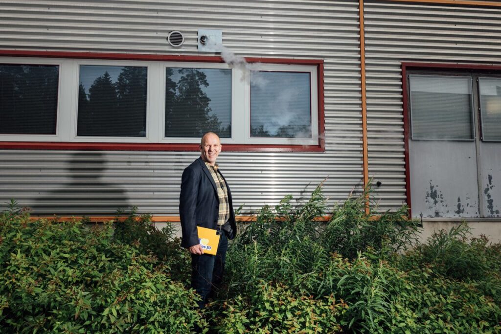
“Tampere will certainly not solve the problem alone, but we are part of a strong European team to tackle critical dependencies, find new opportunities and thus bring competitiveness to Europe”, says Petri Räsänen, Director of the Chips from Tampere programme by Business Tampere.
EU Chip Competence Centre and chip pilot line to Tampere
Europe has woken up to the harsh reality and the fact that it needs to develop the chip sector itself in order to break the dependence on China and the United States. At the same time, the wake-up call can lead to a more brilliant future. The Chips from Tampere programme was established in summer 2023. Its aim is to make use of the EU’s Chips Act package and the funding of tens of billions of euros it provides.
The Chips Act aims to strengthen the production and development of semiconductors, i.e. microchips, in Europe. The aim is to double Europe’s share of the world chip market from the current 10% to 20% by 2030.
Finland has also published its own Chips from the North strategy, the aim of which is to triple the turnover of semiconductor companies operating in Finland. At the same time, the number of employees is estimated to increase from the current 7,000 to as much as 20,000.
But let’s get back to Tampere. Under the leadership of the Tampere Chip Programme, the Finnish Chips Competence Centre (FiCCC) has already been established in Finland to accelerate the digitalisation of industry and other sectors with the help of chip technology. Its headquarters are located on the Tampere University Campus Arena. The EU wants a similar centre of excellence in each member state.
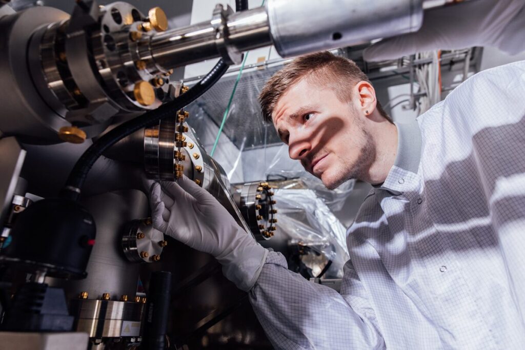
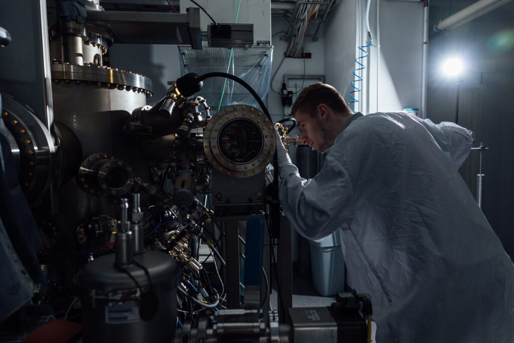
In addition to the Competence Centre, the Chips from Tampere programme will also create a SiPFAB pilot line in the city, which can be used to develop and test new chip systems in co-operation with companies. There are only five similar pilot lines in Europe. They aim to strengthen Europe’s pioneering role in chip technology.
The Tampere pilot line is part of the development and research of so-called third-generation semiconductors in Europe. “Silicon carbide and galium nitrite semiconductors are used, for example, in power electronics or radio frequency applications”, says Tuomas Lahtinen, Director of the SiPFAB pilot line from the University of Tampere. “In practice, this means, for example, that in electric vehicles, electricity must be converted to be compatible with the battery, the transformer uses power semiconductor components. The same applies to wind or solar power.
Tampere focuses on the packaging and integration of these components. The pilot line is a significant step for the chip expertise in Tampere and Finland”, says Lahtinen.
Up until now, the work in Tampere has been more focused on the material and equipment sector. We are now expanding our packaging and integration capabilities. SiPFAB co-operates with companies, but researchers and research groups also have access to our technologies and thus we are also able to develop new innovations.
Design is the core of chip competence
An estimated 8,000 chip design professionals work in the EU. More than 500 of them, or more than six per cent, are in Tampere. The University of Tampere has played a strong role in both developing current chip expertise and training future chip experts.
Semiconductor technology has been developed in Tampere for over 40 years, and the university has also been invited to participate in the development of the EU design platform. Planning is the most economically viable area of the chip value chain and it also requires the most expertise.
“The top expertise in chip design was originally created for Nokia’s needs. Training of experts started way back in the 80s, and Nokia’s communicator was the world’s first smartphone. There is extensive co-operation with various research institutes and companies”, says Räsänen.
The new pilot line can, for example, be used to experiment with new chip integration and packaging methods. Combining, integrating and protecting chips have a significant impact on chip performance and value.
As an example, Räsänen mentions electric cars, where chips must withstand high voltages and currents. Meanwhile, batteries should preferably decrease in size. However, for current materials, the temperature produced by the chip may be so high that it will damage the chip. New materials can improve the durability of chips and reduce waste heat.
Another example is artificial intelligence.
“If we talk about the chips required by artificial intelligence, at the moment the limitation is not so much computational power but data transfer. New materials can be used to speed up and facilitate telecommunications and inter-chip collaboration while improving energy efficiency. Improving reliability in tasks requiring high computing power and energy is very important.
So far, the pilot line is still in the start-up phase. “The construction of clean rooms is expected to begin in 2026, and the first projects are expected to start in summer 2027”, says Tuomas Lahtinen, Director of the pilot line. The aim is for 15–20 people to work on the pilot line.
Using chips to protect top secret information?
The University of Tampere and companies have also had a joint research centre, SoC Hub, which, as its name suggests, has focused on System-On-Chip co-creation, for example, the current needs of 6G networks, artificial intelligence or the security sector.
A new NextSoC project is pending as a follow-up to the SoC Hub. Here a long-term Tampere-based company Insta will also join the co-operation.
The 65-year-old Insta, who employs 1,200 people, specialises in encryption technology for defence, central government and public authority information. In Finland, the information and documents of the authorities and central government are classified according to the level of security. Secret information must also remain confidential.
Insta’s telecommunications encryption systems are used in both public authority and civilian sectors. The systems are approved not only by the Finnish authorities but also by NATO and the EU.
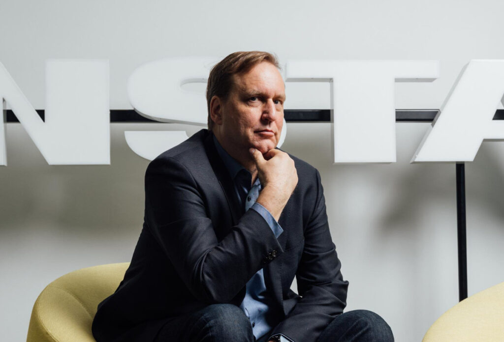
“For a long time, data protection has been software-based. However, it is no longer enough for higher security classifications, and the protection must be implemented with physical components”, says Tatu Männistö, Technology Director of Insta Advance Cyber Security Solutions. At worst, errors in software-based solutions can compromise the entire system, while chip-based solutions ensure more predictable behaviour even in the event of errors. This is why Insta is also taking part in chip development.
“Chips improve the security level and reduce the physical size and power consumption of encryption devices, for example. Chips can be used to better prepare for future needs in general, whatever they are. Contingency planning must also be started well in advance”, Männistö explains.
Development into a product requires years of work
Business Finland funding has been applied for NextSoC, which will be implemented in co-operation with companies and the university. Insta’s goal is to use the project to find out what it takes to make the chip needed by the company and how much it costs.
According to Männistö, the threshold for seeking new markets would be significantly higher without the chip ecosystem in Tampere.
“It is a big factor that there are operators like this in Finland that also pave the way for companies. It is also good for the university that companies like us that have industrial requirements and wishes related to the characteristics of chips, such as safety mechanisms and performance, can join. Things are not made simply because the know-how exists, but because they meet the needs of the market.
Insta’s long-term goal is to exploit the commercial potential of chip-based protection and increase competitiveness in international markets.
The development work is long-term. It may take years for any new products to be on the market. The projected research will take three years, and at the end of the project, we might see how we could commercialise it, how long it takes to mass produce it and so on.”
The safety sector also requires public authority evaluation, which might take some time. Although the chip sector and technological development are progressing rapidly, Männistö also sees positive aspects in the scope of the authorities’ certification processes.
“In information security, conservativeness can be considered a good thing. Old technology is more well-known and won’t cause surprises when it is certified and on the market. If we used top development products, we might come across surprises considerably more often.”
Competition in the chip sector is globally fierce. Insta’s Männistö is not afraid of competition, as it is always a sign of opportunities.
“If there are no competitors, there is no business potential. Although defence budgets are growing around the world, our field is rather niche. We do not compete with products that can be purchased online. In the public authority sector, the race is much more mellow.”
More investments in Finland – and Tampere
With the new openings, Tampere aims to multiply the number of chip experts in the city in the future. At the moment, the design of chips in the Tampere region employs more than 500 people, but according to Petri Räsänen from Business Tampere, the number of chips could be up to three times higher in the future. The greatest challenge is the lack of talent across Europe.
“As a university, we play our own part. There is a demand to add chip topics to the university’s curriculum. SocHub already trains their own experts, and I’m sure we’ll be doing it as well”, says Tuomas Lehtonen from SiPFAB.
In addition to experts, there is naturally need for further investments.
“We should keep in mind that chip-related investments are not always in the tens of billions, but there are other kinds of factories, too. On the Finnish scale, hundreds of millions or a billion euros of factory investments can be realistic, and we are constantly striving to engage in discussions with industry on how to get one to Finland and Tampere, says Räsänen.
Tampere is one of Finnish InnoCities. The city’s key areas of innovation development include industrial renewal, buildings, energy and infrastructure, as well as digital health solutions. Emerging focus areas also include chip technology, dual-use technologies, and the international expansion of the startup ecosystem.
Contact us for co-innovation and investment opportunities in Tampere!
- Petri Räsänen, Senior Director, general inquiries, RDI and policy collaboration
petri.rasanen@businesstampere.com - Sampo Härkönen, Development Specialist, business development
sampo.harkonen@businesstampere.com - Oliver Hussey, Head of ICT, investments
oliver.hussey@businesstampere.com
Want to know more Finnish miracles? Subscribe to InnoCities newsletter (published 3-4 times / year) from below!